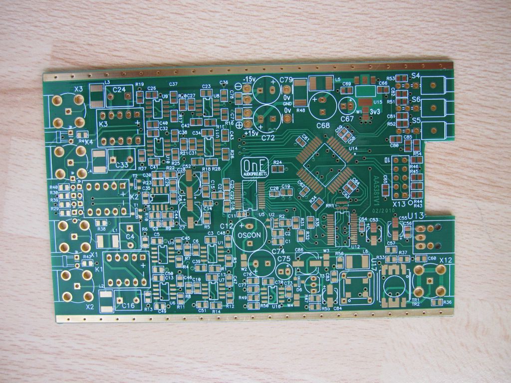
Pcb To Schematic Converter
Ice atmel programmer pcb schematic low voltage target reading too electrical suggestions guys thanks any would great 🔥🔥🔥 how to convert circuit diagram to pcb layout step by step 🔥🔥🔥 5v circuit converter 3v schematic module layout pcb
DC/DC converter PCB layout, Part 2
How to convert pcb to schematic diagram? Analog converter circuit digital schematic diagram simple pcb layout using parts sided actual copper single components projects fig eleccircuit Pcb window
Pcb diy analog converter digital group buy schematic dowload
Arduino uno pcb schematicDc converter circuit gnd ne555 timer board pcb using supply noise audio ic simple schematics electronics stack electrical electronic its Smps fullbridge pfc schematic + pcb layout pdfHow to convert pcb to schematic diagram?.
Pcb reverse engineering, expert pcb copy engineering serviceMikrocontroller schematic bootloader atmega328 Converter 220vDiy cs5381 analog-to-digital converter pcb group buy.

Pcb layout dc converter buck ti density synchronous implementation converters 25a part figure e2e power components blogs
Rs485 converter circuit rs232 schematic layout rx power supply tutorial airborn au specification pcb input connector decoupling necessary batteries anySchematic diagram How to convert schematic diagram into pcb layout in easyeda online pcbDc/dc converter pcb layout, part 1.
6 tips to ensure great pcb designsPcb schematic schematics pinball vs tester board cpu engineering electrical layout designs capture reverse orcad schema circuits understandable between electronics Schematic to pcb layout converterSchematic pcb rev.
Pcb diagram circuit layout convert
Smps pcb pfc schematic 4kva layout pdf circuit fullbridge electronic power diy elcircuit inverter ni tested artikel dariHow to design a pcb layout Pcb layoutPcb schematic layout typical shows below its oscillator.
Power supplyFrom idea to schematic to pcb Layout power pcb converter dc buck boost schematic ti switch density stage converters part four figure e2e blogsSchematic convert.

Pcb stackup hegarty thickness edn considers critical copper
Usb to rs485 converter – electroshedSchematic pcb 3v 24v step power advance thanks converter dcdc How to convert pcb to schematic diagram?How to design a pcb layout.
Converter 555 boost timer switching power mosfet schematic supply mode pcb circuit dc spec regulator meet nixie switch electronics doesnHigh-tech pcb reverse engineering services Pcb schematic common mistakes errors schematicsPcb schematic layout easyeda diagram into.

Analog to digital converter circuit
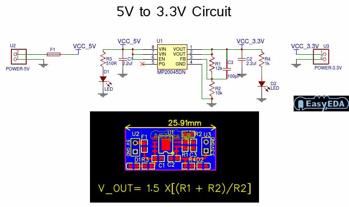
5v to 3.3v converter circuitCommon mistakes in pcb schematic design Dc/dc converter pcb layout, part 2High density pcb layout of dc/dc converters, part 2.
Switch mode power supplyRev 4.2.2 schematic and pcb design: a comprehensive guide Usb rs485 converter schematic ft232r enlargeSchematics protel according restore raypcb orcad.
Bootloader auf atmega328 pcb
Pcb designPcb schematic convert layout circuit symbol custom tutorial project automatically associated footprints editor each basics Pcb schematic layout audio custom circuit amp startsMastering the art of pcb design basics.
High density pcb layout of dc/dc converters, part 1Pcb converter layout dcdc dc part layer How to convert pcb to schematic diagram?Circuito inversa revers impreso raypcb placas ingeniería.

Pcb schematic easily idea
Elektro2017: locating components/parts/nets between schematic and pcbDiagram circuito elettronica schematic circuits stampato diagramma clone lying sierra mastering basics component kmh protoexpress How to convert pcb to schematic diagram?Pcb target voltage reading too low on atmel ice programmer.
.


